The chips are based on IBM's 32nm, Silicon-on-Insulator (SOI) technology, which was jointly developed with GLOBALFOUNDRIES and other members of IBM's Process Development Alliance, with early research at the University at Albany's College of Nanoscale Science and Engineering. The technology vastly improves microprocessor performance in multi-core designs and speeds the movement of graphics in gaming, networking, and other image intensive, multi-media applications. The SOI process was used to build the microprocessor that powered IBM Watson, the question-answering computer that won the Jeopardy! quiz show in early 2011.
"IBM has helped make New York State one of the world's premier locations for semiconductor design and manufacturing," said Michael Cadigan, general manager, IBM Microelectronics. "Recently, we announced that we would spend $3.6 billion researching and developing new silicon technology in New York. We bring the skills, investments and partnerships that keep New York at the forefront of advanced silicon development and manufacturing."
"Today's announcement is a natural extension of our longstanding partnership with IBM that includes production of 65nm and 45nm chips at our fabs in Singapore and Germany," said GLOBALFOUNDRIES CEO Ajit Manocha. "With the addition of our newest factory in New York, we will now be jointly producing chips with IBM at four fabs on three continents."
New York's "homegrown" HKMG technology offers cost-savings, better performance
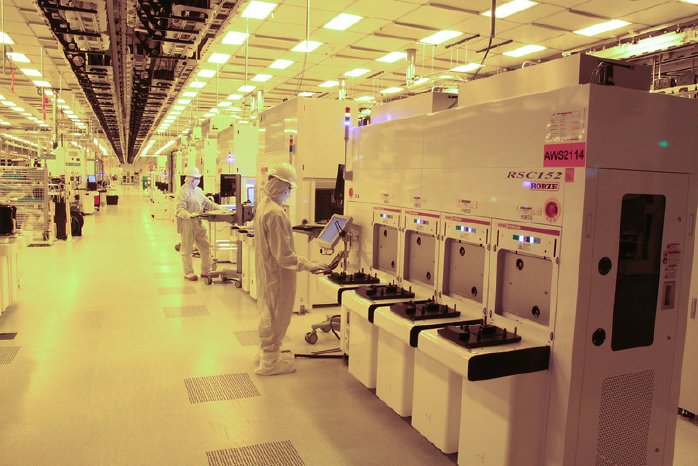
GLOBALFOUNDRIES' new Fab 8 campus, located in the Luther Forest Technology Campus about 100 miles north of the IBM campus in East Fishkill, stands as one of the most technologically advanced wafer fabs in the world and the largest leading-edge semiconductor foundry in the United States. When fully ramped, the total clean-room space will be approximately 300,000 square feet and will be capable of a total output of approximately 60,000 wafers per month. Fab 8 will focus on leading-edge manufacturing at 32/28nm and below.
The companies' 32/28nm technology uses the same "Gate First" approach to High-k Metal Gate (HKMG) that has reached volume production in GLOBALFOUNDRIES' Fab 1 in Dresden, Germany. This approach to HKMG offers higher performance with a 10-20% cost saving over HKMG solutions offered by other foundries, while still providing the full entitlement of scaling from the 45/40nm node.
The new chips also will feature IBM's eDRAM (embedded dynamic random access memory) technology, which dramatically improves on-processor memory performance in about one-third the space with one-fifth the standby power of conventional SRAM (static random access memory). IBM chips are at the heart of the company's server and storage systems, the world's fastest supercomputers and many of the best-known and widely used communications and consumer electronics brands.
ABOUT GLOBALFOUNDRIES
GLOBALFOUNDRIES is the world's first full-service semiconductor foundry with a truly global manufacturing and technology footprint. Launched in March 2009 through a partnership between AMD [NYSE: AMD] and the Advanced Technology Investment Company (ATIC), GLOBALFOUNDRIES provides a unique combination of advanced technology, manufacturing excellence and global operations. With the integration of Chartered Semiconductor in January 2010, GLOBALFOUNDRIES significantly expanded its capacity and ability to provide best-in-class foundry services from mainstream to the leading edge. GLOBALFOUNDRIES is headquartered in Silicon Valley with manufacturing operations in Singapore, Germany, and Saratoga County, New York. These sites are supported by a global network of R&D, design enablement, and customer support in Singapore, China, Taiwan, Japan, the United States, Germany, and the United Kingdom.
For more information on GLOBALFOUNDRIES, visit http://www.GLOBALFOUNDRIES.com.
